
Core Announcement and Key Specifications
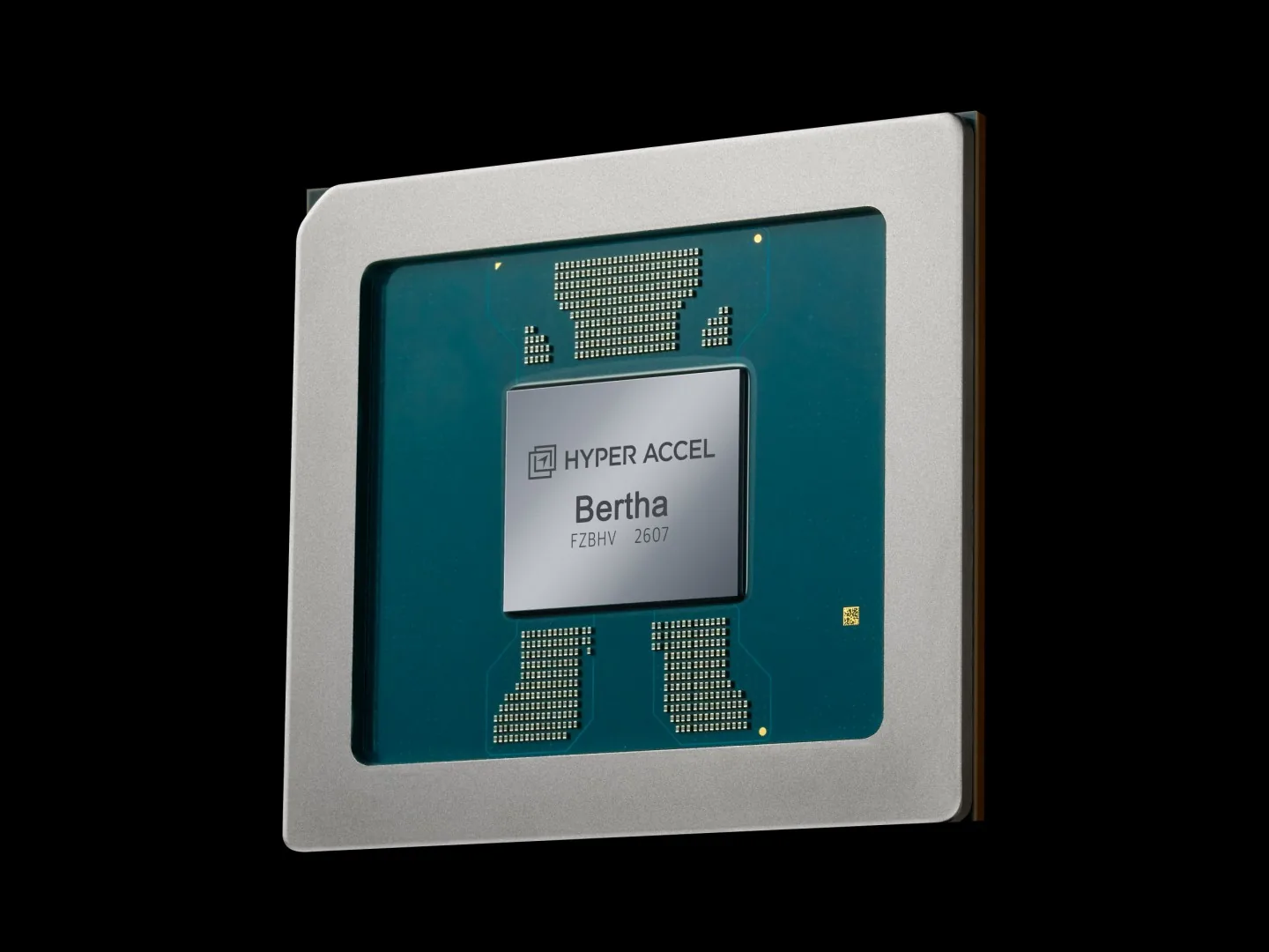
South Korean AI chip startup HyperAccel has announced the mass production of its Bertha data center AI inference accelerator chip on Samsung’s 4nm process node. The news was officially released by semiconductor design service provider SEMIFIVE on September 8, 2026.
- Production Start: September 8, 2026
- Process Node: Samsung 4nm
- Die Size: 500mm² (corresponds to Bertha 500 model)
- FP8 Compute Performance: 768 TFLOPS
- Data Type Support: FP16/FP8/FP4, INT8/INT4
- On-Chip Cache: 256MB SRAM
- Off-Chip Memory: 128GB or 256GB LPDDR5X (546GB/s bandwidth)
- Thermal Design Power: 250W TDP
- Form Factor: Dual-slot PCIe AIC
Technical Specifications and Design Insights
The Bertha 500, designed for data center deployment, features hardware optimized specifically for inference workloads. The 256MB on-die SRAM cache combined with up to 546GB/s memory bandwidth aims to mitigate data movement bottlenecks common in AI inference scenarios. LPDDR5X, while offering lower bandwidth than HBM memory, provides better cost efficiency and power performance—ideal for inference workloads with more moderate bandwidth requirements.
A key claimed advantage is dual focus on throughput and energy efficiency. HyperAccel states the Bertha 500 achieves 2x throughput, 19x better cost效益 (cost-effectiveness), and 12x better energy efficiency compared to NVIDIA H100. The “energy efficiency” metric refers to compute per watt, while “cost-effectiveness” likely combines unit price and adjusted for efficiency.
An notable counterpoint is the 500mm² die size paired with 768 TFLOPS FP8 performance. In advanced nodes, this compute density suggests a design prioritizing high computational unit density over the massive memory bandwidth required for training chips, contrasting with training accelerators that often exceed 1000mm² with HBM3 memory.
Product Line Strategy and Market Positioning
HyperAccel employs a dual-product strategy:
| Product Model | Deployment Target | Reported Die Size | FP8 Compute |
|---|---|---|---|
| Bertha 500 | Data Center Inference | 500mm² | 768 TFLOPS |
| Bertha 100 | Edge Device Deployment | Not disclosed | Not disclosed |
The dual-slot PCIe AIC form factor enables deployment in existing server racks without custom chassis design, lowering migration barriers for data center customers. The 250W TDP falls within the typical range for inference accelerators (NVIDIA L4: 72W, L40: 300W), balancing performance with cooling feasibility.
Reader Recommendations
Recommended for:
- Cloud providers and internet companies needing high-volume AI inference with strict throughput requirements
- Organizations facing NVIDIA H100 shortages or high pricing seeking alternatives
- Data center operators prioritizing compute-per-watt efficiency metrics
** advisable to wait**:
- Users tied to CUDA ecosystem who need framework compatibility verification
- Those conducting large model training workloads—the chip is explicitly marketed as an inference accelerator with no stated training capability
- Applications requiring extreme memory capacity beyond 256GB, as the maximum configuration is 256GB LPDDR5X
Final Thoughts
Bertha’s mass production marks South Korea’s first实质性 (tangible) step into the AI chip sector. By targeting the relatively mature inference segment, HyperAccel avoids the extreme bandwidth and complex interconnect requirements characteristic of training chips, reflecting a pragmatic technical approach. If the claimed efficiency and cost advantages withstand market validation, Bertha could meaningfully reshape the competitive landscape of data center AI acceleration.